HOME

HOYA CANDEO OPTRONICS CORPORATION

 
Information Laser System / Equipment UV Products Electro Optical Glass Campany Profile
HOME > Products Opto-Electronics Glasses > SD-2: Silicon to Glass Bonding Wafers

Electro Optical Glass

Products Opto-Electronics Glasses

Laser System / Equipment
UV Products
Electro Optical Glass
Products Colored Glass Filters
Products Opto-Electronics Glasses
SD-2: Silicon to Glass Bonding Wafers
Standard Specification
Inspection Equipment
Software
Inquiry
CATALOG

MSD-2: Silicon to Glass Bonding Wafers

HOYA's SD-2 substrate is designed with a coefficient of thermal expansion curve which closely matches Si single crystal.

Thermal Expansion Properties
  Borosilicate glass has been widely used as a bonding material to Silicon Wafer. CTE curves of Borosilicate glass and Silicon Single Crystal Wafer cross at about 240°C. When anodic bonding is performed at 400°C, the difference of the expansions at high temperature creates residual stress in the Si chip during cooling to room temperature. As precision of LSI circuit patterning moves to less than 0.25 microns, distortion between the silicon and glass wafers becomes a critical issue.

HOYA's SD-2 substrate is engineered to minimize the distortion or bowing effect caused by the thermal mis-match between the two wafers.

Download the SD-2 : Silicon to Glass Bonding Wafers Brochure (1MB)

Anodic Bonding
  Silicon and glass wafers are generally put together by way of Anodic Bonding. This bonding is formed when positive (+) DC voltage is applied to the Si wafer and negative (-) is applied to the glass wafer while the wafers are pressed and heated. During the bonding process, a small amount of Na+ ions, engineered into SD-2, move as electroconductive carriers to facilitate a very short bonding time.


Features
 
  • Matching CTE to Si Wafer
  • No Phase Separation
  • Optimized for Anodic Bonding
  • Reduced Fresnel Diffraction
  • High Flatness Mask
  • High Young's Modulus
Applications
 
  • Silicon Wafer Bonding
  • Photolithography
  • Pressure Sensors
  • Displacement Sensors
  • Semi Conducto


Thermal Properties
SD-2 Borosilicate
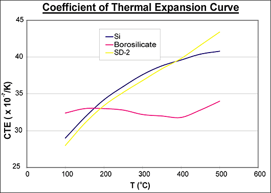
Coefficient of Thermal Expansion 32.0x10⁻⁷/°C 32.5x10⁻⁷/°C
Transformation Point (Tg) 721°C 552°C
Sag Point (Ts) 787°C  
Strain Point 669°C 510°C
Annealing Point 720°C 560°C
Thermal Conductivity 0.0026 Cal/sec·m°C 0.0027 Cal/sec·m°C
Specific Heat 0.176 Cal/g°C 0.180 Cal/g°C
Mechanical Properties
SD-2 Borosilicate
Specific Gravity 2.60 2.23
Young's Modulus 8860 kgf/mm2 6400 kgf/mm2
Modulus of Rigidity 3560 kgf/mm2  
Poisson's Ratio 0.244 0.200
Knoop Hardness 638 kgf/mm2 418 kgf/mm2
Electrical Properties
SD-2 Borosilicate
Volume Resistivity (DC500V) 20°C 4.1 x 10¹⁴ Ω·cm 1.4 x 10¹⁶ Ω·cm
Volume Resistivity (DC500V) 100°C 4.2 x 10¹¹ Ω·cm 4.6 x 10¹¹ Ω·cm
Volume Resistivity (DC500V) 200°C 3.8 x 10⁹ Ω·cm 0.9 x 10⁹ Ω·cm
Dielectric Coefficient (1MHz) 20°C 6.0 4.8
Dielectric Coefficient (1MHz) 100°C 7.0 4.9
Dielectric Coefficient (1MHz) 200°C 7.0 5.1
Dielectric Loss (1MHz) 20°C 1.0 x 10⁻² 5.5 x 10⁻³
Dielectric Loss (1MHz) 100°C 1.9 x 10⁻² 1.0 x 10⁻²
Dielectric Loss (1MHz) 200°C 4.9 x 10⁻² 2.9 x 10⁻²
Chemical Properties
SD-2 Borosilicate
Acid Durability
(30% HNO3 80°C 50H)
1.20 mg/cm2 loss 0.50 mg/cm2 loss
Alkaline Durability
(0.01N NaOH 50°C 15H)
0.01 mg/cm2loss 0.02 mg/cm2loss
Optical Properties
SD-2 Borosilicate
Refractive Index (nd) 1.531 1.474
Abbe-Number (vd) 59  
   
  Note: The listed data are standard value. Because of continuous product improvement, the various data listed are subject to change without notice.