|
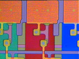
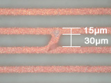
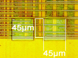
| TFT panel Before cutting |
 |
|
 |
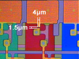
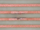
| TFT panel After cutting |
 |
|
|
|
|
|
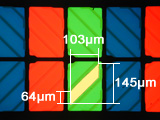
| TFT panel Before cutting |
 |
|
|
| TFT panel After cutting |
 |
|
|
|
|
|
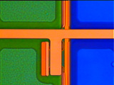
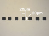
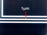
| PC board Before cutting |
 |
|
|
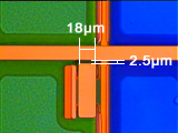
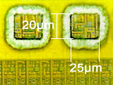
| PC board After cutting |
 |
|
|
|
|
|
| O-LED |
 |
|
|
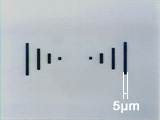
| Expose bottom layer of IC |
 |
|
|
|
|
|
| Exfoliation of protection layer for IC |
 |
|
|
| Color filter processing |
 |
|
|
|
|
|
| Cr film processing |
 |
|
|
| Point markings of analysis |
 |
|
|